This website requires Javascript for some parts to function propertly. Your experience may vary.

Boundary Scan (IEEE 1149.1) | STAR ELECTRONICS

Boundary Scan (IEEE 1149.1): A Complete Guide for Hardware Validation

Boundary Scan, standardized under IEEE 1149.1, has become a cornerstone technology for validating and testing complex electronic boards - such as FPGAs, PCBs, or Ethernet-based systems - without the need for direct physical access. For engineers working with high-density boards and limited probing possibilities, Boundary Scan and JTAG (Joint Test Action Group) offer a non-intrusive and standardized method to detect interconnection faults, verify components, and debug hardware designs effectively.

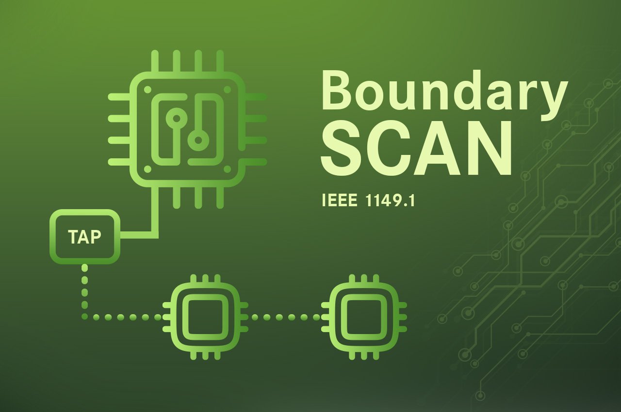
What is Boundary Scan?

Boundary Scan was developed as part of the IEEE 1149.1 standard to address the challenges of testing modern boards with fine-pitch components and multi-layer designs, where traditional bed-of-nails testers or physical probes are impractical.

The concept is simple yet powerful: it integrates a test architecture within the chip itself, allowing signals to be injected, monitored, and analyzed at the pin level via a serial interface - typically using JTAG.

How does Boundary Scan work?
  • Boundary Scan Cells (BSCs): Each I/O pin of the device includes a boundary scan cell capable of capturing and shifting test data

  • Test Access Port (TAP): A dedicated interface (with pins TDI, TDO, TMS, and TCK) controls data flow into the scan chain

  • JTAG Controller: A software or hardware interface that drives test instructions and reads responses, enabling fault detection and board-level validation

Using this chain of scan cells, engineers can isolate faults like open circuits, shorts, or misaligned connections - without powering up the full system or using intrusive probes.

Why Boundary Scan is essential for Automotive and FPGA Boards
  • Non-intrusive testing: Crucial for dense designs with inaccessible pins

  • Accelerated debugging: Detects interconnection faults faster than traditional methods

  • Scalability: Works across multi-board systems, reducing complexity during validation

  • Reliability: Ideal for automotive-grade boards where safety and precision are critical

For Ethernet-based systems, Boundary Scan also allows validation of PHYs, connectors, and signal integrity without requiring live network traffic - ensuring robust hardware before integration into the vehicle environment.

Boundary Scan and JTAG: The Perfect Pair

While Boundary Scan defines the methodology, JTAG provides the communication protocol and the test access interface. Together, they form a standard testing environment that supports:

  • Debugging at the firmware and hardware level

  • In-system programming of FPGAs and microcontrollers

  • Real-time verification during manufacturing or prototyping

Practical Applications
  • FPGA validation: Testing interconnections between FPGA pins and external components

  • Ethernet boards: Verifying signal paths, connectors, and Layer 2 elements

  • Production testing: Automating defect detection before boards enter final assembly

Production at STAR ELECTRONICS uses technologies like Boundary Scan to ensure high quality products that can be used over many years in various projects. With this high quality STAR ELECTRONICS ensures value for customer as well as sustainable and environment friendly investment.

Key Takeaway

Boundary Scan (IEEE 1149.1) enables engineers to validate complex hardware faster and more reliably, reducing costs and avoiding delays due to undetected faults. It is the industry standard for non-intrusive hardware testing - especially relevant for automotive Ethernet and FPGA-based systems.

Glossary

Term

Definition

Boundary Scan

A method for testing interconnections on PCBs without physical probes

IEEE 1149.1

The standard defining Boundary Scan architecture

JTAG (Joint Test Action Group)

Protocol and interface used for Boundary Scan and in-system programming

TAP (Test Access Port)

Interface with control pins (TDI, TDO, TMS, TCK) for accessing scan chains

BSC (Boundary Scan Cell)

Circuit element at each I/O pin used for test data capture and shifting

FPGA (Field Programmable Gate Array)

Reconfigurable integrated circuit used in embedded systems

PCB (Printed Circuit Board)

Physical board that connects electronic components

PHY (Physical Layer Device)

Component responsible for Ethernet signal transmission and reception

In-system programming

Programming of devices directly on the board without removal

Non-intrusive testing

Testing method that does not require physical contact with signal paths

Contact us

Back to top